

Agile-Chip is a method for developing chips quickly and at low cost, currently under development at the X-NICS Center for Innovative Semiconductor Technology Democratization.
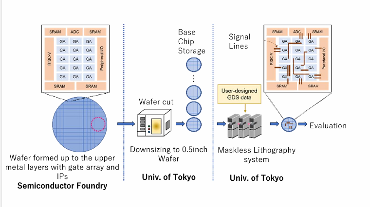
As shown in the figure, RISC-V, SRAM, I/O, and the gates of the gate array are implemented using up to the fourth metal layer of a 0.18 μm 1P6M process, and these are cut out in the form of a 0.5-inch wafer. By forming the wiring on this wafer using Minimal Fab, an SoC can be constructed in approximately 30 minutes.
The APCCAS 2026 Agile-X Chip Design Contest uses this design environment to build original analog and digital SoCs, and participants will compete based on the originality of their ideas and the quality of their designs. Participants must have access to a design environment provided by VDEC or similar organizations, including Cadence Virtuoso, Cadence Innovus, and Siemens Calibre. After registration, the PDK, design flow, and instructional videos will be distributed. Participants are expected to study these materials, complete their designs by the deadline, and submit the GDS file together with a one-page abstract, in the same format as the APCCAS 2026 Demo Session. Entries selected as outstanding through the review process will actually be fabricated using Minimal Fab, packaged, demonstrated at APCCAS, and awarded prizes. Participants will be able to observe the fabrication process at Minimal Fab, and the fabricated chips will be provided free of charge.
For details, please visit our website: https://www.agile-x.t.u-tokyo.ac.jp/en/
Schedule
June 1: Application deadline; distribution of the PDK and design flow
July 1: Submission of GDS files and abstract papers
July 31: Notification of selected outstanding design
August: Chip fabrication and bonding
September: Distribution of the demonstration environment
October 25–28: Demonstrations and award ceremony at APCCAS
If you have any questions,
hunga-at-dlab.t.u-Tokyo.ac.jp