

List of Scheduled Tutorials
1. Bridging the Gap Between Design and Simulation of Analog/RF ICs: The ACM Model

Deni Germano Alves Neto (Université Grenoble Alpes, France and Federal University of Santa Catarina, Brazil)
Deni Germano Alves Neto (Graduate Student Member, IEEE) received the B.S. degree in electronics engineering and the M.Sc. degree in integrated circuits and systems from the Federal University of Santa Catarina (UFSC), Florianópolis, Brazil, in 2018 and 2022, respectively. He participated in a year-long exchange program at Worcester Polytechnic Institute, Massachusetts, USA, in 2014/2015. He conducted ultra-low-voltage/ultra-low-power IC design as a research assistant in the Integrated Circuits Laboratory at UFSC. He is pursuing a joint Ph.D. between UFSC and Université Grenoble Alpes, France, in the TIMA laboratory. His Ph.D. research includes analog/RF and open-source IC design and the development of an advanced compact MOSFET model for IC design and simulation. He has participated in several open-source IC design initiatives: the 2021 and 2023 SSCS PICO Contest, and the 2023-2025 UNIC-CASS. He is also the author/co-author of articles that won the NEWCAS 2023 Best Paper Award and the best student paper at LASCAS 2026.
Abstract
The design of analog and RF integrated circuits depends critically on how the IC designer understands and exploits the characteristics of the MOS transistor. In modern industrial design flows, accurate verification is performed using highly parameterized compact models such as BSIM and PSP, which are indispensable for final validation but provide limited physical insight during the early sizing phases of IC design, precisely where trade-off analysis and informed design decisions are most critical. At the opposite end of the spectrum, the piecewise textbook MOSFET models lack the accuracy and continuity required to address modern technology nodes and fail to describe the weak- moderate-inversion regions in which low-voltage/low-power circuits operate.
This tutorial is based on the Advanced Compact MOSFET model (ACM), a design-oriented charge-based MOSFET model that captures device behavior across all regions of operation, from weak to strong inversion and from triode to saturation, through a single-piece description of the drain current. The model is built on only five physical parameters: the threshold voltage VT0, the specific current IS, the slope factor n, the drain-induced barrier lowering coefficient sigma, and the velocity-saturation parameter zeta. ACM is implemented in Verilog-A and runs unmodified in both the open-source ecosystem (Ngspice) and proprietary EDA flows (Spectre). Both the Verilog-A code and a differential-evolution-based parameter extractor are publicly available. A central theme of this tutorial is the use of ACM as a design-oriented abstraction layer that complements industrial compact models rather than replacing them. Attendees will learn how to extract ACM parameters from silicon measurements (IHP SG13G2 130 nm open BiCMOS PDK) or directly from a foundry models, how to couple the ACM equations with Python scripts to automate biasing and sizing through gm/Id and inversion-coefficient methodologies, and how to benchmark the resulting designs against foundry PDK simulations. The methodology is illustrated through the design and simulation of representative analog building blocks and a resistive-feedback RF LNA, with ACM-based design results compared side-by-side against the foundry PDK model.
The tutorial concludes with a forward-looking module on a wafer-specific, design-oriented ACM model for RF circuits. In advanced nodes, process variation propagates non-linearly into circuit performance and is conventionally addressed through corner/Monte-Carlo analysis. Building on a recent methodology validated in 28 nm FD-SOI CMOS, this module shows how the parametric-test (PT) data routinely collected on every production wafer can be mapped, through a regression, onto the ACM DC parameters, the parasitic capacitances, and the excess channel-noise factor of a fabricated device. The result is a per-wafer, simulation-ready ACM model card delivered as a Verilog-A component, suitable for post-fabrication RF analysis (gm, fT, channel noise) without any additional test structures or measurement overhead — turning the design-oriented ACM model into a practical vehicle for variability-aware RFIC design.
7F Conf Room B, Half-day (13:30-15:00 & 15:30-17:00, Oct 25)
2. Network Quantization for Efficient AI Systems: Algorithm-Hardware Co-design
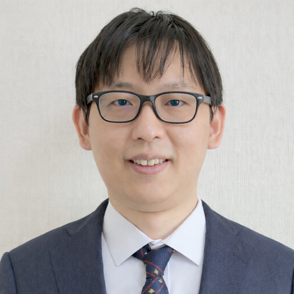
Heming Sun (Institute of Science Tokyo, Japan)
Dr. Heming Sun (M’17–SM’25) received the B.E. degree from Shanghai Jiao Tong University, and the M.E. degree from Waseda University and Shanghai Jiao Tong University. He received the Ph.D. degree from Waseda University in 2017. He has held positions as a Researcher at NEC Central Research Laboratories, an Assistant Professor at Waseda University, and an Associate Professor at Yokohama National University. He is currently an Associate Professor at Institute of Science Tokyo.
His research interests include algorithms and VLSI architectures for video compression and neural networks. He has received several awards, including the IEEE Circuits and Systems Society (CASS) Visual Signal Processing and Communications (VSPC) Rising Star Award. Dr. Sun has also delivered a tutorial at ISCAS 2021 on topics related to learned image and video compression. He has been serving as the IEEE CASS VSPC-TC Membership Subcommittee Chair since 2021, and is currently an Associate Editor for IEEE Transactions on Circuits and Systems for Video Technology (TCSVT) and a Guest Editor for IEEE Journal on Emerging and Selected Topics in Circuits and Systems (JETCAS).
Abstract
Neural networks have achieved remarkable success across a wide range of applications. However, their deployment is increasingly constrained not only by computational cost but, more critically, by memory bandwidth limitations. As modern models continue to scale, data movement between on-chip and off-chip memory has become a dominant performance bottleneck, posing significant challenges for efficient system implementation.
Network quantization has emerged as an effective approach to alleviating these challenges by reducing numerical precision and improving both computational and memory efficiency. By converting 32-bit floating-point (FP32) representations to low-bit formats, quantization can significantly reduce energy consumption and bandwidth requirements. However, this efficiency gain comes at the cost of degraded numerical accuracy, leading to a fundamental trade-off between algorithmic performance and system efficiency.
In recent years, substantial progress has been made in both quantization-aware training (QAT) and post-training quantization (PTQ). In particular, PTQ has become the dominant solution for large-scale models such as large language models (LLMs), where retraining is often impractical. At the same time, emerging challenges including activation outliers, memory-intensive inference, and hardware constraints have driven the development of new quantization strategies.
This tutorial provides a system-oriented perspective on network quantization, covering both algorithmic principles and hardware implications. We first introduce the fundamentals of quantization and review QAT and PTQ techniques. We then discuss quantization in modern large-scale models, with an emphasis on practical challenges and design trade-offs. Finally, we explore algorithm-hardware co-design, highlighting how quantization interacts with compute throughput and memory hierarchy. The goal of this tutorial is to provide practical insights for designing efficient neural network systems under real-world constraints.
6F Room 607, Mini Tutorial (13:30-15:00, Oct 25)
3. Low-Power Frequency Reference: Architectures, Design, and Stability Trends
Ka Meng Lei (University of Macau, Macau)
Ka-Meng Lei received the B.Sc. degree in Electrical and Electronic Engineering from the University of Macau in 2012, and the Ph.D. degree in Electrical and Computer Engineering from the same University in 2016. He has been with the University of Macau since 2019 and is currently an Associate Professor. He was a Postdoctoral Fellow at Harvard University from 2017 to 2019, where he was involved in developing the high-resolution portable nuclear magnetic resonance (NMR) spectrometer.
Ka-Meng Lei has published 60+ refereed papers, including 7 papers in the IEEE ISSCC proceedings and 13 in the IEEE JSSC. He co-authored three books and two book chapters in Springer. His research interests include precision analog circuits, frequency references, sensors and analog front-end interfaces, and high-resolution portable NMR/Magnetic Resonance Imaging platforms. He has been a Technical Program Committee member of ISSCC since 2026 and ICTA since 2021. He is currently serving as the Associate Editor of IEEE Open Journal on Circuits and Systems and IEEE Transactions on Biomedical Circuits and Systems.
Abstract
As the demand for ubiquitous sensing and “always-on” connectivity grows, the frequency reference—an indispensable module for defining the timescale—has emerged as a critical bottleneck in the design of energy-efficient systems. Achieving high-frequency stability while maintaining a micro-to-pico-watt power profile requires a deep understanding of the fundamental trade-offs among noise, physics-based drift, and circuit topologies. This Tutorial provides a comprehensive exploration of the state of the art in CMOS frequency reference, bridging the gap between traditional quartz-based solutions and modern fully integrated references.
The first part of the Tutorial focuses on CMOS Crystal-Based Reference, detailing emerging low-power circuit architectures that push power down to the sub-nanowatt regime while exploiting the crystal’s robust frequency accuracy to maintain stable oscillation across process and temperature corners. The second part transitions to Integrated CMOS References, including open-loop (e.g., relaxation oscillators, ring oscillators, etc.) and closed-loop (frequency-locked loop) RC-based oscillators. We will discuss the design challenges inherent in these integrated solutions, specifically the trade-off between temperature coefficients and power consumption.
Finally, the Tutorial also discusses emerging calibration strategies such as crystal-/inductor-assisted calibration necessary to achieve sub-1 ppm/°C stability without 32-kHz resonators. Attendees will gain a clear perspective on selecting the optimal frequency reference architecture for diverse application requirements, from high-precision communication to low-power sleep timers.
6F Room 607, Mini Tutorial (15:30-17:00, Oct 25)
4. Towards Batteryless IoTs: Power Management Interface Circuits for Kinetic Energy Harvesting

Madhav Pathak (Indian Institute of Technology Gandhinagar, India)
Madhav Pathak received the B.Tech. degree in electrical engineering from Indian Institute of Technology (IIT) Roorkee India, in 2016, and the Ph.D. degree in electrical engineering from Iowa State University, Ames, IA, USA, in 2022. In December 2023, he joined the Indian Institute of Technology Gandhinagar (IITGN), India, as an Assistant Professor in the Department of Electrical Engineering, where he currently leads the Low-Power Circuits and Systems (LP-CAS) Research Group. His research interests are in ambient micro-power energy harvesting and Power Management IC Design. Dr. Pathak has been the recipient of several prestigious honors, including the IITGN Research Fellowship, NSF-INTERN Award, Honda Young Engineer and Scientist (YES) Award, the DAAD WISE Scholarship, among others.
Abstract
This tutorial spans from the physics of transduction in ambient kinetic energy harvesters to the state-of-the-art Power Management ICs, essential for realizing the next generation of self-powered IoT devices. Firstly, fundamental limits of transducible energy, explaining the distinctions between lightly coupled and strongly coupled kinetic harvesters in simple, intuitive terms will be presented. Next, we revisit the basic circuit models for the three major types of harvesters: piezoelectric, triboelectric, and electromagnetic and their unique requirements for efficient energy extraction. Next, we will take a deep dive in specialized architectures and MPPT strategies suited for Electromagnetic Harvesters low internal impedance. For Piezoelectric and Triboelectric Harvesting, a step-by-step build-up of advanced synchronous switched architectures from first principles will be presented. We will compare multiple available architectures, including the latest state-of-the-art designs (both discrete and on-chip), within a common framework to highlight unique and shared design aspects. Finally, we dwell upon harvester-circuit co-design strategies necessary to reach the fundamental realizable limits of kinetic energy extraction. This session will be enjoyable for power management circuit designers as well as general enthusiasts interested in physics of energy harvesting/transduction.
6F Room 604, Mini Tutorial (13:30-15:00, Oct 25)
5. Architecting Low-Power PLLs: Multi-Loop Strategies for IoT and Automotive Applications
Yann Deval (University of Bordeaux, France)
Prof. Yann DEVAL (M’96, SM’07) joined the University of Bordeaux in the Southwest of France in 1993, as an Assistant Professor, focusing on the design of analog ICs, RFICs, high-speed mixed-signal ICs, and high-reliability electronics. He pursues his research within the IMS, the laboratory of Integration, from Material to System. In 1999, Dr. Deval became an Associate Professor and, in 2004, a Full Professor. From 2006 to 2010, he was the head of the IC Design Group, and from 2011 to 2016 the head of the Devices, Circuits and Systems (DCS) Department. Since 2016, Dr. Deval has been the director of IMS. This public research laboratory is composed of 150 Ph.D. students and 150 faculty members, with the support of roughly 100 technicians, engineers, and admin assistants.
Abstract
Low-power Frequency Generation Units (FGUs) are key enablers of RF systems for IoT, ISAC, and automotive applications with always-on operation, where stringent constraints on power, phase noise, frequency agility, and start-up time apply. This tutorial reviews advanced frequency synthesis architectures, with emphasis on multi-loop approaches that efficiently balance locking speed, spectral purity, and energy consumption. Dual-loop strategies combining coarse and fine control are highlighted for achieving fast settling and low in-band phase noise.
Focus is placed on all-digital PLLs (AD-PLLs) and sub-sampling PLLs (SS-PLLs). AD-PLLs offer scalability, programmability, and seamless digital integration, while SS-PLLs achieve superior phase noise efficiency through direct RF sampling. Key design challenges are addressed at circuit and system levels.
The advantages of SOI CMOS technologies are discussed, particularly body biasing for dynamic tuning and reconfigurability. These architectures target automotive RFICs requiring robust, low-power, and adaptable frequency synthesis.
6F Room 604, Mini Tutorial (15:30-17:00, Oct 25)
6. Return-on-Investment Battery Charger Converters in Energy Harvesting: Circuit Theories and Practical Designs
Toru Tanzawa (Waseda University, Japan)
Toru Tanzawa is a professor in the Graduate School of Information, Production and Systems at Waseda University, Japan, and a Fellow of IEEE. He received his B.S. degree in physics from Saitama University, Saitama, Japan, in 1990, his M.S. degree in physics from Tohoku University, Sendai, Japan, in 1992, and his Ph.D. degree in electrical engineering from The University of Tokyo, Tokyo, Japan, in 2002. In 1992, he joined the Toshiba Research and Development Center, Japan, where he worked on the circuit design of high-density NAND Flash memories and high-speed low-voltage NOR Flash memories for ten years. From 2004 to 2017, he was with Micron Memory Japan, Inc., Tokyo, where he worked on MLC/3D NAND Flash design at the Japan Flash Design Center. From 2017 to 2024, he has been at Shizuoka University, focusing on power management circuits and systems design for energy harvesting.
Abstract
When Internet of Things (IoT) sensing modules are deployed in the field, they communicate with one another or with cloud servers to collect environmental information and help maintain society safety with little or no human intervention. However, the batteries used in these sensor modules need to be replaced periodically. The cost of replacing old batteries with new ones has increased significantly as more sensor modules are deployed globally. Return-on-Investment battery charger converters with energy transducer is a key technology to eliminate battery replacement for decreasing the overall cost of sensor networks. This tutorial covers design fundamentals on switching converters and charge pumps as well as design theories and practical designs for hybrid power systems with batteries and energy transducers, based on Return-on-Investment concept, for highly reliable IoT edge devices.
The tutorial is organized as follows:
- Background: IoT Edge Devices and Energy Harvesting ~ 10 min
- Fundamentals: Low Power Designs on ~20 min
1) Buck converter
2) Boost converter
3) Charge Pumps - Design Theories and Practical Designs ~ 60 min
1) ROI Buck Converter
2) ROI Boost Converter
3) ROI Charge Pump - Summary
The conference attendees in the areas of the following tracks will be interested in the proposed tutorial; Analog Circuits, Bio-Medical Circuits/Systems, Low-Power/Low-Voltage Design, Embedded and Micro/Systems, and Sensors and Sensing Systems.
7F Room 701, Mini Tutorial (13:30-15:00, Oct 25)
7. From Hopfield Networks to Fully Coupled Ising Machine LSIs —Optimization Computation Architectures for the Edge AI Era—
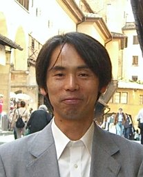
Takayuki Kawahara (Tokyo University of Science, Japan)
Prof. Takayuki Kawahara obtained his BS, MS, and Ph.D. degrees from Kyushu University, Japan. With his MS degree, he joined Hitachi Central Research Laboratory as a research staff member. After leaving the laboratory as a Chief Researcher, in 2014, he became a Professor with the Department of Electrical Engineering, Tokyo University of Science, Tokyo, Japan. Sustainable electronics is the focus of his laboratory, which includes low-power artificial intelligence (AI) devices and circuits, sensors and AI signal processing, spin current applications, and quantum computing techniques. In particular, his achievements in the fully-coupled Ising machine LSI have been highly regarded.
Abstract
As AI systems shift from cloud-centric to edge-based deployment, requirements such as low latency, energy efficiency, and local autonomy become critical. At the core of these demands lies the ability to make optimal decisions, i.e., to efficiently solve combinatorial optimization problems. This tutorial revisits the foundation of such computation, starting from the Hopfield network—one of the fundamental models of modern AI. Its energy minimization principle directly corresponds to the Ising model in physics, forming a natural bridge from algorithm to hardware. This connection leads to Ising machines, which implement optimization processes as physical systems.
This lecture first establishes the relationship between combinatorial optimization and ferromagnetic models, then outlines the evolution from Hopfield networks to Boltzmann machines and modern AI. Based on this foundation, we explain the operating principles of Ising machines and compare major implementations, including quantum annealers, quantum bifurcation machines, optical systems, and semiconductor-based approaches, with respect to cloud and edge usage. The central focus is on fully coupled Ising machine LSI. While physical systems typically rely on local interactions, information processing inherently requires fully coupled interactions among variables. Bridging this gap is essential for practical optimization hardware. This introduces scalable architecture, including dual-scalable and multi-valued spin designs, that enable efficient realization of fully coupled models. These approaches highlight the potential of Ising machine LSI as a low-latency, energy-efficient optimization engine for edge AI.
Outline (90 minutes)
- Introduction: Cloud vs. Edge Computing (5 min)
Overview of the shift from cloud-based processing to edge AI, and the emerging importance of local, low-latency optimization. - Combinatorial Optimization and Physical Models (10 min)
Fundamentals of combinatorial optimization problems and their correspondence to ferromagnetic systems. - From Hopfield Networks to AI (20 min)
Hopfield networks and Boltzmann machines, and their roles as foundational models of modern AI. - Ising Machines: Principles and Implementations (30 min)
Basic operation of Ising machines and comparison of major implementations:
o Quantum annealers
o Optical coherent Ising machines
o Bifurcation machines
o Semiconductor-based Ising machines
Discussion on their applicability in cloud and edge environments. - Fully Coupled Ising Machine LSI (20 min)
Design principles and evolution of fully coupled architectures:
o Scalable architectures
o Dual-scalable configurations
o Multi-valued spin representations - Conclusion (5 min)
Summary and future outlook for optimization-centric edge AI.
7F Room 701, Mini Tutorial (15:30-17:00, Oct 25)
8. Energy-Efficient and Trustworthy CMOS Image Sensing SoCs Based on Sensor-AI and Sensor-PUF Co-Designed Architectures
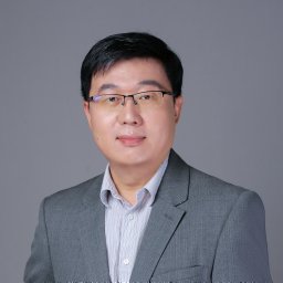
Xiaojin Zhao (Shenzhen University, China)
Xiaojin Zhao (IEEE Senior Member) received the B.Sc. degrees in both microelectronics and applied mathematics from Peking University, Beijing, China, in 2005, and Ph.D. degree in electrical and electronic engineering from The Hong Kong University of Science and Technology (HKUST), Hong Kong, China, in 2010. From 2010 to 2011, he was a Postdoctoral Research Associate with HKUST. In 2012, he joined Shenzhen University, Shenzhen, China, where he is currently a Distinguished Professor with the State Key Laboratory of Radio Frequency Heterogeneous Integration and the College of Electronics and Information Engineering. In 2014, he was a Visiting Scholar with IMEC, Leuven, Belgium. He has published 120 international journal articles and peer-reviewed conference papers (mostly in IEEE). His research interests include CMOS image sensor, gas sensor, and their related trustworthy sensing techniques based on the hardware security primitives of physical unclonable function (PUF) and true random number generator (TRNG).
Abstract
In recent years, inspired by the principles of human vision, dynamic vision sensors (DVS) based on in-sensor computing pixels are attracting more and more research attention due to their advantages in energy efficiency. The DVS is based on the concept of “events” rather than traditional “frames”, so it is also called event-based vision sensor. However, while focusing on the dynamic information in the scene, existing DVS chips automatically filter out a lot of equally useful static information, which has large influence on the accurate recognition and decision by the back-end processing algorithms. In addition, most edge-AI chips are designed separately from the CMOS image sensing chips, and there are few image-sensing SoC designs with the DVS and edge-AI co-designed, in order to achieve more energy-efficient and intelligent recognition. To address above issues, this tutorial will first introduce two image sensing SoC designs: 1) a global-shutter-based dual-mode APS-DVS hybrid imaging sensing SoC with in-pixel adaptive conversion gain; 2) an end-to-end sensor-AI-co-designed image sensing SoC with highly-energy-efficient edge CNN. Moreover, existing CMOS image sensing chips lack an effective root of trust mechanism at the hardware level, and the software-level secure transmission protocols developed to protect the communication channels have also ignored the hardware security vulnerabilities from the edge image sensing terminals. To address the security threats from the emerging generative AI attacks on the generated raw image or video contents, how to implement anti-spoofing technology from the hardware level of image sensing chips has become an urgent issue to be addressed. In response to this issue, this tutorial will also introduce an image sensing SoC design based on in-senor hardware security architecture with an optically-reconfigurable physical unclonable function (PUF).
7F Room 702, Mini Tutorial (13:30-15:00, Oct 25)